Back Heterojunction

Back Heterojunction

Back Heterojunction a-Si:H/c-Si Solar Cells

Schematic diagram of rear side view, gridless front surface and schematic cross section of final device. Doped p+-type and n+-type a-Si:H regions are shrunk to points within the interdigitated grid pattern (picture not to scale).
Crystalline silicon solar cell technologies – front junction, back junction (interdigitated back contact), and a-Si:H/c-Si front heterojunction have grown over the decades and almost matured now. There is a less room for efficiency improvement and/or price reduction.

In the front junction and front heterojunction structure, a limiting performance factor is the inevitable shading losses due to current collecting grids at the light illuminating front side.

Shading losses can be as high as 4%. It can be reduced by making smaller grids. However, this results in an increase in series resistance and consequently a reduction in solar cell performance. A trade-off exists between shading losses and series resistance.
Conventional p-n junction c-Si solar cell technology is used in commercial solar power generation. To form p-n junction, phosphorous diffusion is performed into p-type c-Si for n-type emitter.

Emitter formation by POCl3 diffusion is well established. Pre-diffusion process requires high temperature of ~950°C for more than 20 min. After that, a drive-in dopant process is required around the same temperature for about 20 min that determines p-n junction depth.

Point Contact Structure

Our research group addressed the above trade-off issue by incorporating a new solar cell structure known as point contact back heterojunction (BHJ) structure. Both p+-type and n+-type doped a-Si:H regions lie at the rear side as points. Other research groups have used doped region as line instead of points.

In our BHJ structure, for the first time, we have used interdigitated point contacts instead of interdigitated line contacts (point, line refers to doped area geometry). Point contact structure improve output voltage due to a reduced emitter component of dark current.

BHJ structure allow wider grid structure at the non-illuminating side and resistive losses can be avoided. Thus, trade-off issue can be eliminated. More details can be found from our articles mentioned under references.

Interdigitated point contact BHJ structure combines the advantages and fabrication methods of SANYO type front heterojunction (a-Si:H/c-Si:H) solar cell, and SunPower type back junction c- Si solar cell (interdigitated back contact).

SANYO type is a high Voc technology, maximum processing temperature is around 260°C, and intrinsic a-Si:H is used for surface passivation. A drawback is front grid at the light entering side.

SunPower type is a high Jsc technology. The important feature is gridless front surface, and both p-type and n-type contacts are placed at the rear side in the form of interdigitated pattern. However, an obstacle is that processing temperature can be as high as 1025°C.

BHJ is a combination of above two process technologies, namely, light enters through gridless surface (yields high Jsc), both p-type and n-type contacts are placed at the non-illuminating rear side having interdigitated pattern, and processing temperature is 260°C (low thermal budget).

To reduce recombination at the metal/semiconductor point contacts, doped areas at the rear side are kept between 10 and 20 µm (gives high Voc ). Therefore, potentially a high Voc , and Jsc can be obtained. TCO layer used at the front side in the front heterojunction is not required in BHJ and hence TCO absorption losses in the short wavelength can be avoided.

BHJ Solar Cells Working Principle

A high pure, thinner (bulk lifetime > 2ms, < 180 µm) n-type c-Si wafer is required since the charge carriers generated near the gridless front surface travel across the bulk and reach their respective electrode. When c-Si wafer is thick, an enhanced recombination can occur before reaching the rear side. Charge collection is explained below.
Schematic cross-section of a-Si:H/c-Si back heterojunction solar cell. Photovoltaic junction lies across c-Si/emitter (i.e., n-type c-Si/intrinsic a-Si:H/p+-a-Si:H). To improve holes collection, BSF area (diameter size) is kept smaller than emitter size. Otherwise, holes will have a greater chance to recombine before reaching the emitter.
BHJ cell can be divided into three broad regions, (1) p-type (emitter) collection region, (2) n- type (BSF) collection region, and (3) diffusion region. The cell operates in a high-level injection mode, where the number of photogenerated charge carriers are very large compared to background doping density of c-Si.

Due to concentration gradient, photogenerated charge carriers produced near the front surface diffuse to the rear side until they reach built-in electric field that exist across (n-type c-Si/intrinsic a-Si:H/p+-a-Si:H) the depletion region. These carriers are then separated laterally by the built-in electric field and reach their respective electrodes.

Back surface field (BSF) across the n-type c-Si/intrinsic a-Si:H/n+-a-Si:H interface provides an additional mechanism which reflect (restrict) holes entering n+-a-Si:H and allow electrons to reach n-type contact.

Device Fabrication

Fabrication process is very similar to interdigitated back junction c-Si solar cells (refer back junction c-Si solar cells from R&D key areas in the technology main menu). For BHJ, fabrication process requires four photolithography masks including the masks required for two lift-off processes. Maximum processing temperature is 260°C.

SiN passivation layer, p+-implant and n+-implant used in the back junction cells are replaced by intrinsic a-Si:H, p+-a-Si:H and n+-a-Si:H respectively.

References from our work

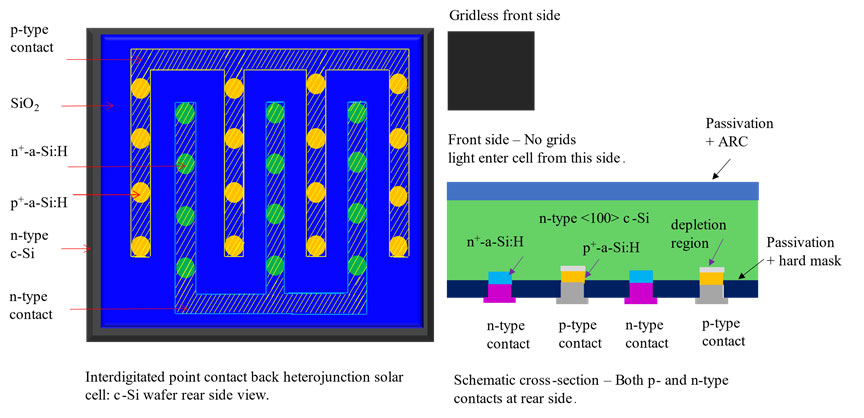
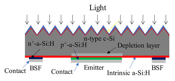
High-efficiency c-Si based interdigitated point contact back heterojunction solar cells
Journal of Materials Science: Materials in Electronics, 28 (2017) 9697–9703.

Two-dimensional simulation studies on high-efficiency point contact back heterojunction (a-Si:H/c-Si) solar cells

Solar Energy, 105 (2014) 109–115.

Influence of emitter bandgap on interdigitated point contact back heterojunction (a-Si:H/c-Si) solar cell performance

Solar Energy Materials & Solar Cells, 109 (2013) 199–203.

Photovoltaic Properties of a-Si:H Films Grown by Plasma Enhanced Chemical Vapor Deposition: A Review

Materials Express, 2 (2012) 177-196.