Perovskite Solar Cells

Perovskite Solar Cells

Schematic cross-sectional diagram of perovskite solar cell. TiO2 (n+) and spiro-OMeTAD (p+) are the commonly used ETL and HTL due to their suitable optoelectronic properties and energy band alignment with perovskite. Light enters through the glass. FTO and metal serve as top and bottom contacts respectively.

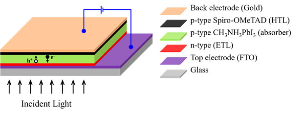
Perovskite based heterojunction solar cells gained enormous attention since their stabilized efficiency is comparable to that of single crystalline silicon (c-Si) solar cells. In the device, perovskite layer is an active light absorbing layer where electron-hole pairs are mainly generated.

Perovskite is sandwiched between electron transport layer (ETL) and hole transport layer (HTL). A planar n+-p-p+ structure consists of Glass/FTO/ETL/Perovskite/HTL/Metal. Perovskite is ambipolar in nature, i.e., it can transport electrons and holes to ETL and HTL respectively.

Perovskite Solar Cells: Working Principle

Lightly doped perovskite layer is completely depleted. A built-in electric field exists across the entire perovskite layer since it is completely depleted. Charge carriers produced in the perovskite are swept away towards their respective electrodes as explained below.

Like c-Si p-n junction, in the ETL/perovskite/HTL (n+-p-p+) solar cell structure, at the n+/p interface, n+-side depletion region contains positively charged donor ions and p-side depletion region contains negatively charged acceptor ions.
Schematic diagram of c-Si p-n junction. Photogenerated electrons from the p-side are attracted by positively charged (depletion layer) donor ions and reach n-side. Similarly, holes from n-side are attracted by negatively charged (depletion layer) acceptor ions and reach p-side. In other words, due to the built-in electric field and since there is no external bias, electrons from p-side drifting to n-side and holes from n-side drifting to p-side, i.e., when there is no external bias, electrons move against the direction of electric field and holes move in the direction of electric field.
In the absence of external bias, since electric field direction is from positive charge (donor ions) to negative charge (acceptor ions), a built-in electric field at the n+/p interface points from ETL (n+) to perovskite (p).

Charge collection at the ETL/perovskite (n+/p) interface

Incident light enters the device through glass/FTO and generates free electron-hole pairs in the perovskite layer. Photogenerated charge carriers in the perovskite move from the bulk towards the interfaces due to concentration gradient. As mentioned above, built-in electric field across the n+/p interface points from ETL to perovskite.

In the unbiased condition, at the ETL/perovskite interface, built-in electric field drift electrons (drift is defined as the movement of charges under the influence of electric field) from perovskite to ETL and repel holes towards the perovskite bulk.

In other words, positively charged donor ions present at the n+-side depletion region attract electrons and repel holes. Hence, only electrons can cross from perovskite to ETL and collected by n-type electrode (FTO). Note that since there is no external bias, electrons drift opposite to the direction of built-in electric field.

Charge collection at the HTL/perovskite (p+/p) interface

The other side of the interface is p+/p (HTL/perovskite). This p+/p interface is like high-low (highly doped/low-doped) junction used close to the rear surface of n+-p-p+ type c-Si solar cells to reduce rear surface recombination (n+, p and p+ represent highly doped c-Si emitter, low doped bulk p-type c-Si, and highly doped rear surface of c-Si respectively).

The electric field across the high-low junction is known as back surface field (BSF). It is used to repels minority carriers towards bulk and lets majority carriers to cross BSF to reach back contact.

BSF across high-low (p+/p) junction points from perovskite to HTL. At the p+/p interface holes are the majority carriers. BSF reflects/repels minority carriers (electrons) towards perovskite bulk and lets the majority carriers (holes) to reach HTL and collected by bottom electrode.

Note that at the high-low (p+/p) junction also, in the unbiased condition, holes drift along the direction of electric field and electrons drift opposite to the direction of electric field.
Simulated energy band diagram of planar perovskite solar cell. Conduction band discontinuity ΔEc1 is negligible. Huge conduction and valance band discontinuities ΔEc2 and ΔEv1 blocks electrons and holes entering HTL and ETL respectively. Valance band discontinuity at the HTL/absorber interface (ΔEv2) is the limiting factor for holes collection efficiency. ΔEv2 of 0.29 eV has been observed for CH3NH3PbI3 absorber bandgap of 1.52 eV. For high collection efficiency, ΔEv2 should be negligible or minimum (< 0.3 eV).

Charge collection interpretation: Using energy band diagram

ETL and HTL are better known as blocking layers for holes and electrons respectively. As shown in the energy band diagram, holes move to HTL; for high collection efficiency, valance band discontinuity at the HTL/perovskite interface must be less than 0.3 eV.

If any holes moving to perovskite/ETL interface do not enter ETL due to a huge valance band discontinuity at the perovskite/ETL interface; it acts as barrier, i.e., ETL blocks holes entering it.

In the conduction band, due to the downhill path, electrons easily reach ETL easily from perovskite layer. A high conduction band discontinuity at the HTL/perovskite interface blocks electrons entering HTL. These two transport layers are known as blocking layers for minority carriers.

Selected References (from our work)

Performance evaluation and optimization of CH3NH3PbBr3 based planar perovskite solar cells using various hole-transport layers
Solar Energy 236 (2022) 832 – 840.

Methylammonium lead bromide based planar perovskite solar cells using various electron transport layers
Solar Energy 221 (2021) 456 – 467.

Influence of Electron Transport Layer (TiO2) Thickness and Its Doping Density on the Performance of CH3NH3PbI3-Based Planar Perovskite Solar Cells
Journal of Electronic Materials 49 (2020) 3533 – 3539.

Effect of absorber layer, hole transport layer thicknesses, and its doping density on the performance of perovskite solar cells by device simulation
Solar Energy 196 (2020) 177 – 182.

Interface studies by simulation on methylammonium lead iodide based planar perovskite solar cells for high efficiency
Solar Energy 190 (2019) 104 – 111.