Copper Indium Gallium Selenide (CIGS) Based Solar Cells

CIGS Solar Cells

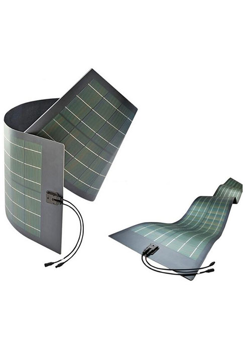
CIGS solar cell technology is an alternate to silicon (Si) solar cell technology and module efficiency is comparable. There are several significant benefits in using CIGS technology..

  • CIGS solar cells are less susceptible to heat than Si solar cells.

  • Due to the direct bandgap nature of CIGS, absorption co-efficient of CIGS (105/cm) is an order of magnitude higher than Si (104/cm) having indirect bandgap.

  • Production involves less raw materials and less time. Maximum processing temperature is around 550°C and energy payback time is about 1 year. Corresponding values for Si cells are around 1100°C and ~2 years.

  • CIGS absorbs most part of solar spectrum within 1 µm, a thin layer of about 2 µm is sufficient for the device. Whereas in Si cells, for high absorption and mechanical strength, wafer thickness ~180 µm is required. About 50% of production cost is due to wafer cost.

  • Light management can be done effectively for high Jsc . High energy photons ≥ 2.42 eV are absorbed by CdS buffer layer (bandgap of CdS is 2.42 eV) and low energy photons (< 2.42 eV) are transmitted and absorbed by CIGS layer.

  • CIGS solar cells can be monolithically integrated during cell processing. In Si solar cells, monolithic integration is not possible.

Device structure and working principle

For CIGS solar cells fabrication two types of device structures are used, (i) substrate structure, and (ii) superstrate structure. In the former, opaque substrates are used and, in the latter, a transparent glass substrate is used, and light enters through glass.

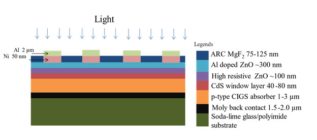
Schematic cross-section of CIGS solar cells having substrate structure. Heterojunction is formed at the p-type CIGS/n-type CdS interface. Top and bottom contacts are Al/Ni and molybdenum respectively. A high resistive intrinsic ZnO layer is used to prevent shunting path due to diffusion of aluminum into the absorber from Al-doped ZnO layer. For lateral conduction of photogenerated electrons to Ni/Al grids, a low resistive Al-doped ZnO is used.

In the substrate structure, light enters through TCO and then enter CdS layer which transmit light up to 2.4 eV to the CIGS absorber layer where charge carriers are mainly produced. High energy photons (≥ 2.4 eV) are absorbed by the CdS layer and charge carriers are created. A built-in electric field is formed across the p-n junction at the p-type CIGS/n-type CdS interface.

A depletion layer is created around the p-n junction due to immobile charges. At the depletion layer, since positively charged donor ions are at the n-side (refer perovskite solar cell page in the technology menu R&D key areas) and negatively acceptor ions are at the p-side, built-in electric field points from n-side to p-side, i.e., from positive charge to negative charge.

In the unbiased condition, built-in electric field drifts photogenerated electrons from absorber layer (CIGS) to buffer layer (CdS). Similarly, holes drifted from buffer layer to absorber layer. Note that electrons drifted opposite to the direction of electric field and holes drifted in the direction of electric field.

It can also be stated that electrons are attracted by depletion layer positively charged donors and moves from CIGS to CdS. Holes are attracted towards depletion layer negatively charged acceptors and moves from CdS to CIGS. Thus, charges are collected at their respective electrodes. Finally, from n-type electrode, electrons travel through the load, reach the absorber, and recombine.

As long as the illumination is on, photogenerated carriers are created again, separated by built-in electric field, electrons travel through load, enter the absorber, recombine and the process continue.

Also, there is an additional mechanism called back surface field (BSF) in the CIGS layer close to the Mo back contact created by a Ga gradient. BSF reflects electrons towards p-n junction and restricts it from reaching Mo back contact.

Since BSF at the rear side of CIGS points from CIGS to back contact, BSF drift holes to reach the back contact, but not the electrons. Because electrons drifted opposite to the direction of BSF, and holes drifted in the direction of BSF. Therefore, electrons created in the absorber close to Mo back contact do not reach Mo back contact.

Challenges to be Solved

  • Since CIGS is quaternary, film composition uniformity over a large area must be solved.

  • If both vacuum and non-vacuum processes (i.e., chemical bath deposition of CdS) are used, substrate handling between tools is an issue.

  • After laser scribing for monolithic integration, cleaning is an important aspect.

  • Graded CIGS bandgap profile slows down the throughput.

  • For large-scale production in large areas, standardization of equipment (uniform performance) for multi-source evaporation and two-stage selenization process are required.

  • At present, 2-3 µm thick CIGS layer is used with deposition time of about 60 min. For industrial production, without deteriorating device performance, 1 µm thick CIGS in about 10 min deposition time is required for high throughput.

References from our work

Book Chapter – Copper Indium Gallium Selenide Solar Cells in “Thin Film Photovoltaics: Single-Junction and Tandem” book edited by
Jeyakumar Ramanujam and Jatin Kumar Rath, Published by Elsevier in 2024.

Flexible CIGS, CdTe and a-Si:H based thin film solar cells: A review

Prog. Mat. Sci., 110 (2020) 100619 (20p).

Copper indium gallium selenide based solar cells – a review

Energy Environ. Sci., 10 (2017) 1306 – 1319.

Electrochemical preparation and characterization of copper indium diselenide thin films

Mat. Res. Bulletin, 29 (1994) 195 – 202.