Front Junction c-Si Solar Cells

Front Junction c-Si Solar Cells

Harnessing the sun, powering a brighter future

Silicon based solar cells, particularly c-Si p-n junction cells dominate the current market. Conventional methods increase the production cost. An alternative method is required to minimize the cost of production. Highly efficient cells with a low-cost production method are required.

Conventional Method

Conventional p-n junction c-Si solar cell technology is used in commercial solar power generation. To form p-n junction, phosphorous diffusion is performed into p-type c-Si for n-type emitter.

Emitter formation by POCl3 diffusion is well established. Pre-diffusion process requires high temperature of ~950°C for more than 20 min. After that, a drive-in dopant process is required around the same temperature for about 20 min that determines p-n junction depth.
Schematic diagram of n+-p-p+ type c-Si solar cell having aluminum back surface field (picture not to scale).
The back surface field (BSF) is formed by screen printing of aluminum paste at the rear side followed by RTP. BSF restricts minority carriers from reaching the rear surface. It repels minority carriers (here, electrons) towards the bulk, increases J sc and reduces rear surface recombination.

The cost versus efficiency ratio is high for conventional p-n junction solar cells due to high thermal budget (defined as area under the temperature versus time curve), number of sophisticated processing steps, low throughput etc.

The other technologies such as a-Si:H solar cells and polymer solar cells have lower fabrication costs, but it comes with lower performance.

Spin-on Low-cost c-Si Solar Cells with Comparable Efficiency

Low-cost refers to $/Wp , where Wp refers to power output under ideal conditions (25°C, light intensity 1000 W/m2). Lowering $/Wp means reducing the numerator by using cheap processes – lower-grade Si feedstock and Si wafers, cheaper dopants, and inexpensive metallization schemes or increasing the denominator by producing highly efficient cells or both.

Spin-on Doping: Simultaneous Emitter (p-n junction) and BSF Formation

We have developed a spin-on doping method to spin-coat phosphoric acid and boric acid as n-type and p-type dopants for simultaneous n-type emitter and BSF formation at the front side and rear side respectively.

Low-temperature curing followed by low-thermal budget RTP for simultaneous emitter (p-n junction) and BSF formation require much less time than diffused p-n junction solar cells.

Boron BSF performs better than aluminum BSF. A high recombination velocity of 600 cm/s and a poor back surface reflectance of 60% is reported for Aluminum BSF.

Boron solubility in Si is higher than aluminum which results in heavy p+-doping at the rear surface and hence a low rear surface recombination. Stress induced bow in thin c-Si wafer can also be avoided by using boron BSF.

The number of processing steps and thermal budget can be reduced by spin-on method. This increases high throughput and decreases cost versus efficiency ratio which makes spin-on doping suitable for industrial mass production.

Front Junction p-type c-Si Solar Cells Working Principle

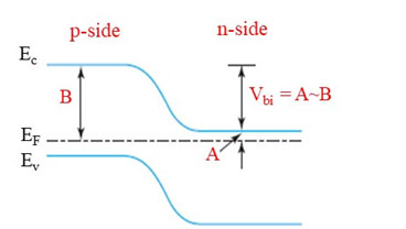
When a p-n junction is formed, a built-in electric field exist across the p-n junction (i.e., across the depletion region) due to negatively charged acceptor ions in the p-side and positively charged donor ions in the n-side (refer perovskite solar cells in the technology menu).

The amount of band bending (A~B) is the built-in potential (Vbi) developed across the depletion region.
The built-in electric field at the junction points from positively charged donor ions to negatively charged acceptor ions, i.e., pointing from n-side to p-side (emitter to absorber).

Under illumination, electron-hole pairs are mostly created in the p-type c-Si absorber. Due to electric field at the junction, electrons are drifted (movement of charge carrier under the electric field) from p-side to n-side, and holes are drifted from n-side to p-side, but not the other way round as explained below. Thus, charge carriers are collected at their respective electrodes.

In the un-biased condition and in the presence of built-in electric field, electrons move opposite to the direction of the field and holes move in the direction of the field, i.e., electrons move towards positively charged donor ions, and holes move towards negatively charged acceptor ions.

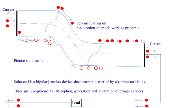
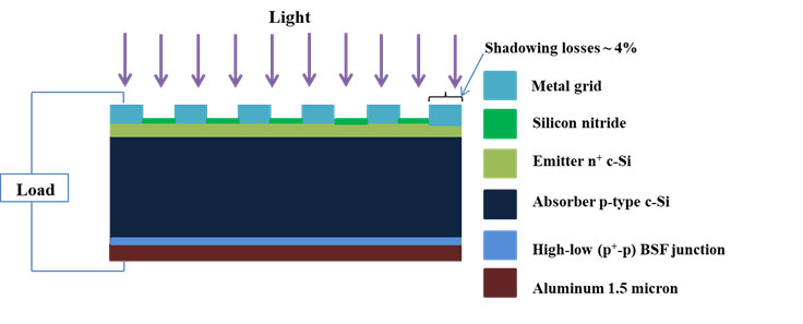
Schematic diagram of charge collection and continuing process as long as the illumination is on.

After charge collection, electrons from emitter flow through the load and reach rear side of c-Si and recombine. If light is continuously on, electron-hole pairs are generated, charges are collected at their respective electrodes, and electrons flow through the load, then recombine with absorber as shown in the above schematic diagram and process will continue.

Back Surface Field

At the rear side of c-Si, BSF provides an additional mechanism. It is formed between highly doped c-Si by aluminum at the rear side and low doped p-type c-Si bulk. BSF is also known as high-low junction. A built-in electric field across the BSF junction points from bulk to rear side (lightly doped p-type c-Si to highly doped p+-region).
The p-p+ junction keeps minority carriers (electrons in this case) in the lightly doped region and away from back contact.
BSF drifts minority carriers (electrons) towards bulk and reduces rear surface recombination. Majority carriers cross through BSF and reach p-type electrode. BSF role is to improve carrier collection (Jsc) in the device and to enhance Voc by lowering recombination at the rear surface.

References from our work

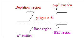
Fabrication of c-Si solar cells using boric acid as spin-on dopant for back surface field
R. Soc. Chem. Adv. 4 (2014) 4225-4229.

c-Si solar cells formed from spin-on phosphoric acid and boric acid

Renewable Energy, 80 (2015) 80-84.

Surface passivation of boron emitters on n-type c-Si solar cells using silicon dioxide and PECVD silicon oxynitride stack

RSC Advances, 6 (2016) 70040-70045.

Electrical and optical characterization of SiOxNy and SiO2 dielectric layers and rear surface passivation by using SiO2/SiOxNy stack layers with screen printed local Al-BSF for c-Si solar cells

Current Applied Physics, 18 (2018) 107-113.

Surface Passivation Schemes for High-Efficiency c-Si Solar Cells - A Review

Trans. Electr. Electron. Mater. 16 (2015) 227-233.

Inorganic photovoltaics - Planar and nanostructured devices (Review Article)

Prog. Mat. Sci. 82 (2016) 294-404.