Ion implantation is a low temperature process used for p-type and n-type doping at the rear side of c-Si wafers to fabricate back junction c-Si solar cells. Doping uniformity of less than 1% variation can be achieved. Dopant concentration, penetration depth and spread range are better controlled than diffusion method used for c-Si solar cells.
Before going to actual fabrication, several process simulations were performed to determine an ideal ion beam energy and implant dose which determines junction (implant) depth and dopant concentration respectively.
Device Fabrication
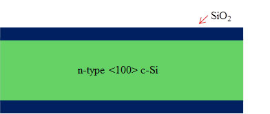
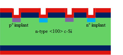
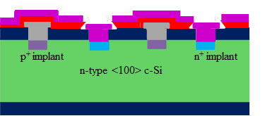
Process sequence is given below for ion implanted back junction solar cells. Process requires four masks. Photoresist and SiO2 were used as soft masks and hard masks. Device dimensions are not mentioned in the schematic diagram and picture is not to scale.
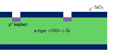
Silicon dioxide (SiO2) deposition.
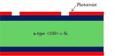
Mask 1: Photoresist spin coated and patterned at the top side. After that, photoresist spin coated at the rear side to protect SiO2 from etching.
SiO2 etched at the top side.
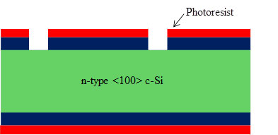
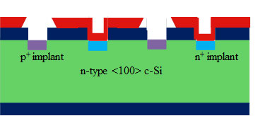
Using SiO2 as hard mask, p+ implanted and resist removed.
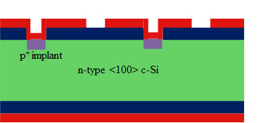
Mask 2: Photoresist spin coated and patterned at the top side for n+ implantation.
Exposed SiO2 etched and n+ implanted.
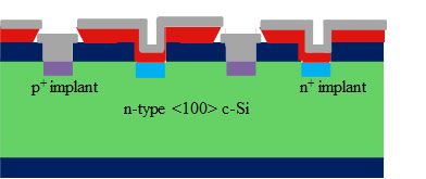
After implantation, resist removed.
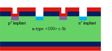
Now, resist coated on both sides. Photoresist is required at the rear side to avoid process induced damages.
Mask 3: Patterned at the front side for metal deposition. While developing, acetone remove the resist in the unexposed areas.
Metal deposited ~0.5 μm.
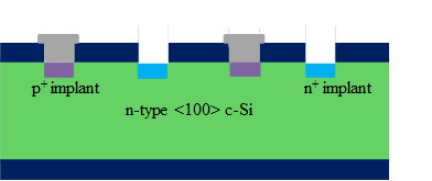
After lift-off photoresist, p-type metal contact is completed.
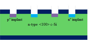
Mask 4: Resist coated and patterned for n-type contact.
Lift-off resist and metal over the resist. Now n-type metal contact completed.
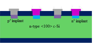
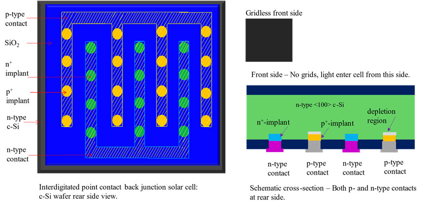
Back Junction c-Si Solar Cells Working Principle
Light enters the device where there are no current collecting grids. Photogeneration occurs near the front side. Charge carriers move to rear side due to concentration gradient. Front surface recombination also occurs.
At the rear side, depletion region and photovoltaic junction exist across n-type c-Si/p-type implant interface. Since the built-in electric field in the depletion region is pointing from n-type c-Si to p+-type implant, it lets holes to reach p+-type implant and do not let electrons to reach p+-type implant.
The back surface field (BSF) is across the n-type c-Si/n+-type implant interface. BSF allows majority carriers (electrons in this case) to cross it and restricts minority carriers. Therefore, electrons are collected by n-type electrode.
Due to gridless front surface, Jsc is enhanced since there are no shadowing losses. For the conventional device with grids at the light incident side, shadowing losses are about 4% (i.e., underneath metal grid, no charge carriers are created).
Reference from our work
Inorganic photovoltaics - Planar and nanostructured devices (Review Article)